15 Common Mistakes in Designing Prototype PCBs and How to Avoid Them
Designing and testing prototype PCBs (Printed Circuit Boards) can feel like solving a giant puzzle. If you’ve ever struggled with electronics projects, chances are you’ve faced some of the pitfalls mentioned below. Let’s break down these common mistakes in simple terms so you can avoid them and save yourself hours of frustration.
Also, Check – Why Isolation Matters in PCB Design? Role of Cutouts in PCB Isolation.
1 ) Sticking to Stale Breadboards

Breadboards are great for quick tests and learning how circuits work. But they’re unreliable for long-term or complex projects. Connections loosen, wires pop out, and over time, your project becomes a mess of broken circuits. Instead of relying on breadboards for months, transition to a proper PCB for a more stable and long-lasting solution.
2) Messy DIY PCB Etching
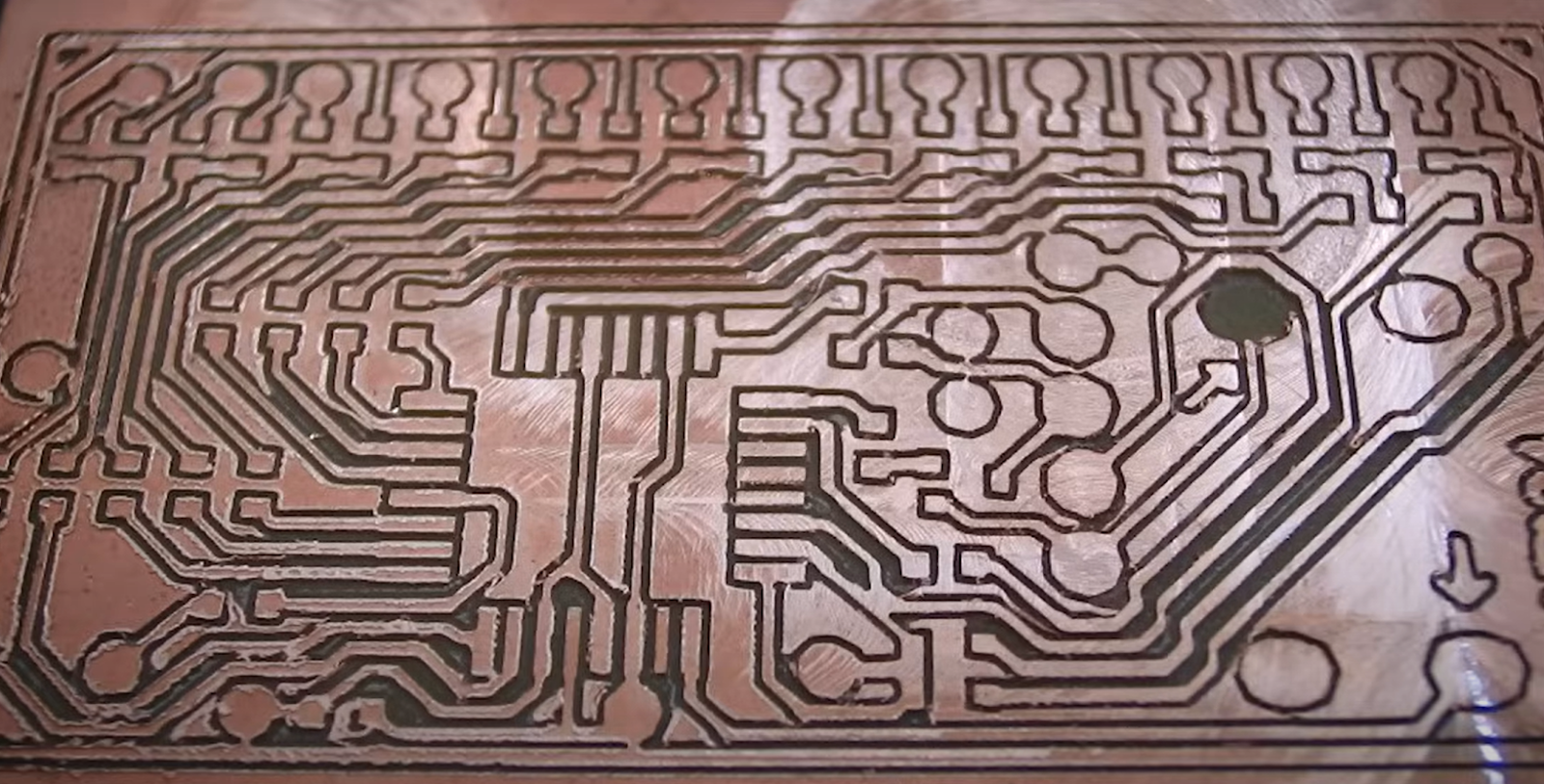
Making your own PCBs at home might seem fun, but it’s usually not worth the trouble. DIY methods are messy, involve chemicals, and can’t handle modern, tiny components. Plus, today’s electronics industry favors small, leadless chips that are impossible to use with old-school methods. For just a few dollars, services like JLCPCB or PCBWay can deliver professional-grade boards in a week—no mess required!
3) Designing for Production Too Early

Many first-time designers try to create a “perfect” PCB on the first attempt, but this rarely works. Prototype PCBs are meant to test and troubleshoot your design, not go straight to production. Make your first board larger than necessary, test all functionalities, and shrink it down later. Use the affordable PCB services mentioned earlier to experiment without breaking the bank.
4) Skipping Test Points in PCB
Without test points (small exposed pads for attaching probes), debugging becomes a nightmare. Imagine trying to attach a probe to a tiny chip leg while hunting for issues. Add test points for key signals like power, ground, and communication lines. They’ll save you time and headaches.
5) No Diagnostic LEDs in the PCB

A simple power or diagnostic LED can make your life easier. It can show whether your board is powered, your battery is charging, or your microcontroller is active. These little lights act as your PCB’s status updates and can quickly pinpoint issues without a multimeter.
6) Overcrowding Components in PCB Design

While it’s tempting to cram everything onto a tiny board, it’s a mistake during prototyping. Leave extra space around components for testing, replacing, or modifying them later. Use slightly larger parts like 0805 resistors and capacitors during the prototype stage to make handling easier.
7) Ignoring the Silk Screen on PCB

The silk screen is the text and markings on your PCB that guide assembly. Clear labeling of components, pin orientations, and test points is crucial. Skipping this step can lead to assembling components backward or wasting time double-checking datasheets. Use text big enough to read (at least 2mm tall) and avoid covering it with other parts.
8) No Isolation Jumpers in PCB

Mistakes happen in new designs, and sometimes you’ll need to disable part of the circuit to troubleshoot. Isolation jumpers, like small removable resistors, let you cut off power to specific sections without removing entire components. This makes debugging much smoother.
9) Forgetting to Break Out Extra GPIOs in PCB


Most microcontrollers have unused pins (GPIOs), which can come in handy if you need to fix or add something later. Break these out to test pads or headers. It’s a small effort during design that can save you from redesigning your PCB.
10 ) UART Pin Confusion in PCB design


Serial communication (UART) is a common feature in PCBs, but it’s easy to mix up transmit (TX) and receive (RX) pins. Always double-check your datasheets and consider adding jumper options to swap pins if needed. This tiny step can save you from hours of debugging.
11) Fixed I²C Addresses

Check Article here
https://ai.thestempedia.com/docs/evive/evive-technical-specifications/arduino-core-interface/i2c-communication/
Some I²C devices have fixed addresses, and if two devices share the same address, they won’t work together. To avoid this, add solderable resistors or jumpers to change the address when necessary. This flexibility is especially helpful for troubleshooting or adding new parts.
12) Combining Power and Main PCBs

If your design includes a power circuit (like voltage regulators), consider separating it from the main PCB. That way, if there’s an issue with the power, you don’t have to throw away your whole board. Use perforations or “mouse bites” to make breaking apart the boards easy.
13) Using Unmarked Resistors in PCBs

Many modern surface-mount resistors lack visible markings, making it hard to verify their values. For prototyping, choose resistors with printed labels, so you can identify and test them without guesswork.
14) Wrong Footprints in PCB design

Not all components fit perfectly into standard PCB footprints. Always compare your component’s datasheet with the dimensions in your design software. A small mismatch can make your part unusable and force you to redesign.
15) Overlooking Part Availability
Even the best design is useless if the parts are unavailable. Check for stock before finalizing your design. It’s a good idea to order critical components ahead of time, especially during shortages.
Designing prototype PCBs is all about planning, testing, and learning from mistakes. By avoiding these common pitfalls, you can make the process smoother, faster, and less frustrating. Remember, prototyping is a journey—don’t rush to the finish line without proper testing.
Check the YouTube Video – Top Fifteen Mistakes People Make When Designing Prototype PCBs
FAQs on Mistakes in Designing Prototype PCBs and How to Avoid Them
1. Why should I avoid breadboards for complex projects?
Breadboards are unreliable for long-term use due to loose connections and their fragile nature. They’re great for small tests but unsuitable for complex or multi-week projects.
2. Can I use a DIY PCB etching method for modern components?
Not recommended. Modern components are too small for DIY methods, and professional PCB manufacturing services are affordable and much more reliable.
3. Why do I need test points on my PCB?
Test points make it easier to probe and debug your PCB without damaging components or soldering wires temporarily.
4. How can diagnostic LEDs help?
Diagnostic LEDs provide quick feedback on power and activity, saving you from troubleshooting basic issues with multimeters.
5. What’s the advantage of breaking out unused GPIOs?
Unused GPIOs can be repurposed for fixes, additional features, or external modules without requiring a redesign.
Happy Learning!